
Semiconductor
Semiconductor Industry:
Sealing Innovation for Ultra-Clean Performance
What are the current challenges for seals in semiconductor applications?
Semiconductor production demands ultra-clean environments. Seals have to perform reliably without contaminating sensitive processes. Depending on the manufacturing process, additional resistance to aggressive chemicals, high temperatures, plasma exposure or high vacuum conditions is necessary.
Ongoing technological progress leads to shrinking chip designs and increasing throughput. Therefore, seals and their materials need to be more durable, low-outgassing and chemically stable. Close collaboration between equipment and sealing experts with high-performance elastomer and thermoplatic sealing solutions are key to meet these evolving demands.
Process Steps and Applications in the Semiconductor Industry – From Lithography to End Effector Solutions
Semiconductor manufacturing involves a highly intricate value chain, where each process step imposes specific demands on materials and components. A fundamental distinction can be made between several core process categories, each with unique environmental and operational challenges that directly impact the selection of sealing solutions:
- Wet chemical processes including wafer cleaning, wet etching, and photoresist development typically involve corrosive acids, bases, and solvents. Sealing materials used here must offer exceptional chemical resistance and maintain high purity to prevent contamination.
- Thermal processes such as oxidation, diffusion, and annealing operate at elevated temperatures, often above 300 °C, in controlled atmospheres. Seals in these environments must withstand thermal cycling, maintain mechanical integrity, and exhibit minimal outgassing.
- Plasma processes, including plasma etching and Plasma-Enhanced Chemical Vapor Deposition (PECVD), expose components to reactive ionized gases. These conditions require seals with high plasma resistance and low particle generation to ensure process stability and yield.
- Vacuum-based processes such as sputtering, Atomic Layer Deposition (ALD), and Chemical Vapor Deposition (CVD) demand seals that maintain vacuum integrity over extended periods. Low permeability, minimal extractables, and high cleanliness are further critical performance criteria.
Selecting the right sealing solution is not merely a matter of material compatibility; it requires a deep understanding of the process environment, equipment design, and contamination control requirements. The following section provides an overview of representative applications within the semiconductor industry.

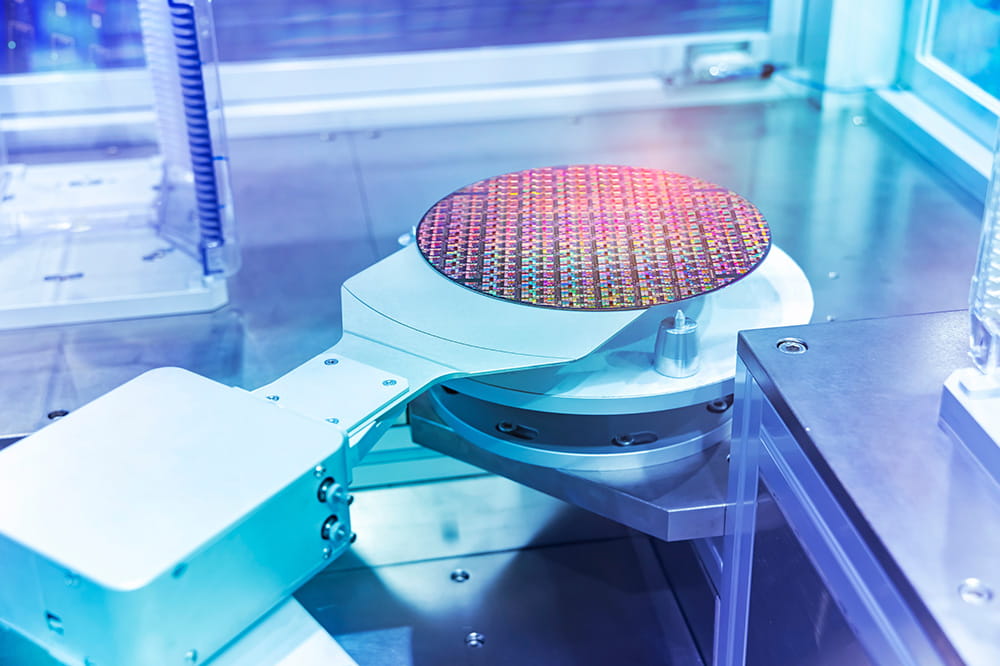
Lithography
Lithography is one of the most critical and sensitive steps in semiconductor manufacturing. It demands exceptional control over environmental conditions, chemical purity, and mechanical stability. These requirements place unique demands on the sealing materials used in lithography equipment.
As even microscopic particles can cause defects in pattern transfer, seals must be produced from ultra-clean materials and exhibit extremely low particle generation. The seals have to be chemical resistant against photoresists, developers and cleaning solvents and avoid leaching or outgassing that could interfere with the process chemistry.
As pattern sizes shrink with technological development and extreme ultraviolet lithography (EUV) becomes standard, requirements on sealing materials even increase. Long-term reliability is a must.
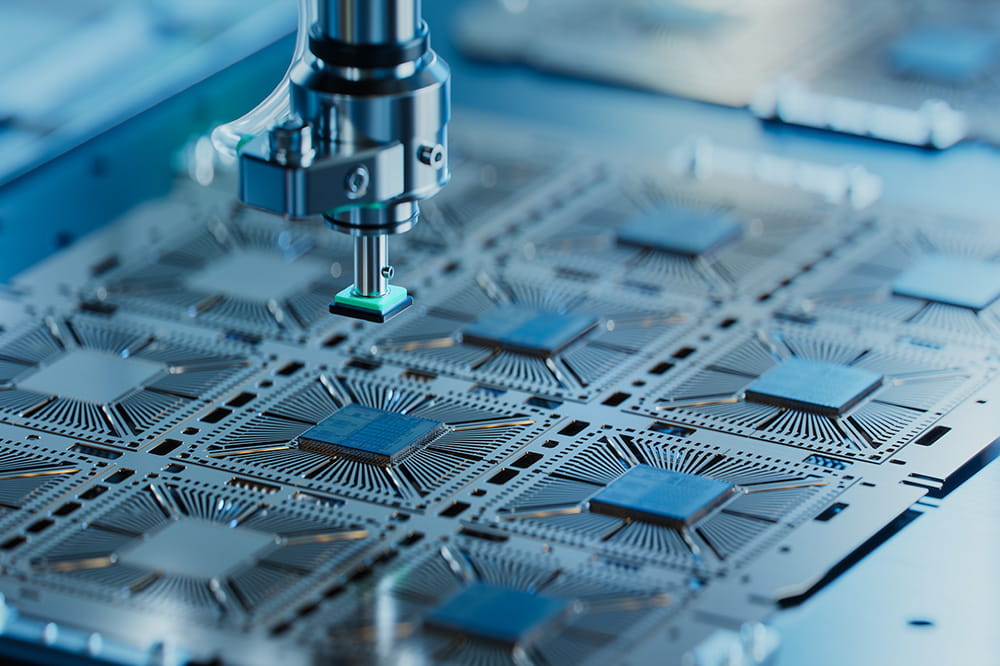
End Effector Solutions
End effectors are important components in semiconductor wafer handling systems that ensure a precise and contamination-free transfer during production. Seals in end effector systems play a critical role in ensuring contamination-free, reliable operation. Low particle generation is mandatory to avoid contamination and damage on wafers. Wafers become thinner and more fragile, which means that end effectors have to provide high accuracy. Sealing materials have to withstand temperature fluctuations and fulfill electrostatic discharge (ESD) requirements. Additionally, they have to resist to cleaning agents and process-related residues without degrade or release of any substances which could interfere with the process.
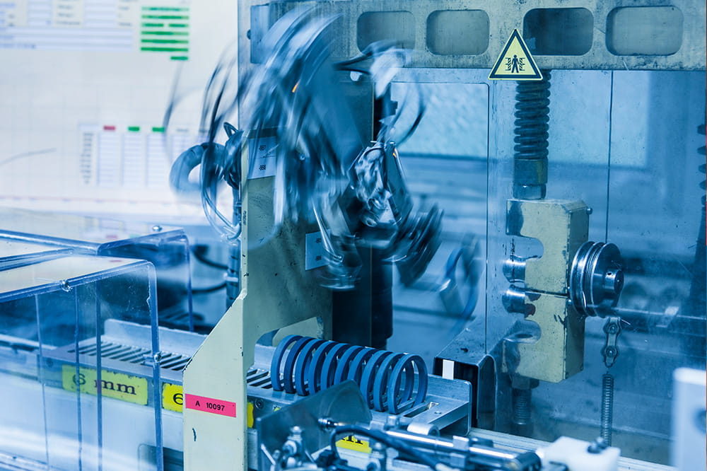
Advanced Packaging
Advanced Packaging in the semiconductor industry refers to techniques used to integrate multiple chips or chiplets into a single, compact, high-performance package. Processes such as die attach, wire bonding, underfill, and encapsulation are extremely sensitive to particle contamination. Seals have to be made from ultra low outgassing materials, in which especially inorganic contamination is critical. They have to withstand organic and inorganic media and avoid leaching or degradation which could interfere with bonding or curing processes. As temperatures usually exceed 250 °C, the seals must be thermally stable for long-term operation. In addition, the sealing materials have to be anti-static to prevent charge buildup and exhibit low friction and minimal wear properties.
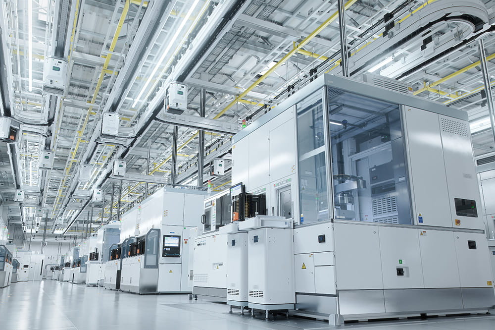
Sub-Fab
The category Sub-Fab refers to the infrastructure supporting the operation of the semiconductor fab. It contains systems for distributing process gases, chemicals, ultrapure water (UPW) and electrical power and is crucial for the process stability, safety and efficiency of the entire fab. Typical components are for example vacuum pumps, abatement systems, connectors of gas and chemical distribution pipes and tubes, heat exchangers, valves and sensors. They all require ultra-clean high-performance sealing solutions that resist extreme operating conditions, such as harsh chemicals and guarantee process purity as well as low outgassing.
Sealing Expertise for Wet Chemical, Thermal, Plasma and other Applications in the Semiconductor Industry – From O-rings to Customized Seals
Sealing Expertise for Wet Chemical, Thermal, Plasma and other Applications in the Semiconductor Industry – From O-rings to Customized Seals
Most of these semiconductor materials are available for standard sealing products like o-rings, but also customer-specific and metal-bonded seals. Different cleanliness classes of finished products are available to meet individual customer requirements.
- 65 FFKM 059905
Yellow coloured next generation ultrapure FFKM material for highest demanding applications. The main advantages are low-outgassing, high temperature and minimum particle release.
- 75 FFKM X75019
White coloured FFKM material that resists high temperatures and offers low outgassing. Proven sealing material, for example for advanced packaging applications.
- 75 Simriz® 486
White coloured FFKM material with excellent plasma resistance, minimum particulation, deposition and metalization. Proven sealing material, for example for chamber lid and window seals as well as gate valves.
- 75 Simriz® 495
Black coloured FFKM material with broad chemical resistance in particular for wet chemical applications. Proven sealing material, for example for vacuum valves and pumps.
- 75 Simriz® 508
Off white coloured FFKM material with outstanding long-term resistance to extreme temperatures in PECVD (Plasma-Enhanced Chemical Vapor Deposition) applications, as well as with optimal high-temperature compression set in remote plasma etching and ashing processes. Proven sealing material, for example for isolator valve seals.
- 80 Simriz® 498
Black coloured FFKM material with high temperature resistance, excellent performance in acids and other harsh chemicals as well as superior long-term performance in virtually all environments.
Additional FKM, FFKM and PTFE materials for dedicated applications are available on request.
Contact us to find the ideal sealing solution for your semiconductor application.
Services for Semiconductor


Join Us!
Experience Freudenberg Sealing Technologies, its products and service offerings in text and videos, network with colleagues and stakeholders, and make valuable business contacts.
Connect on LinkedIn!